How it works
Basic circuits
Basic logic gates are easily constructed with relays and diodes. A
simplifying design rule represents logic "true" signals with a connection
to 5 volts and "false" signals with no connection to anything.
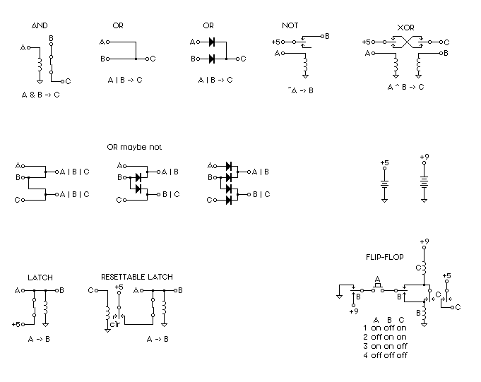
The AND circuit shown in the diagram has inputs A and B that can either
be connected to 5 volts or left unconnected. If both A and B are
connected to 5 volts then the output C will also have 5 volts. Five
volts on terminal A energizes the relay coil, and that closes the reed
switch contacts, making the C output the same as B.
An OR circuit is even simpler. If either A or B is connected to 5 volts
then the output C has 5 volts. Alas, this is too simple for the general
case. As shown in the diagram where two outputs are intended, diodes must
be inserted to get the correct result. When designing circuits, it's a
good idea to always insert the diodes. Unnecessary diodes can be removed
after the design has been correctly worked out.
The NOT circuit is easily implemented using the normally closed contact
on a double throw relay. Five volts on terminal A energizes the relay
coil, which pulls the switch lever toward it and away from the contact
connected to terminal B.
Similarly, the XOR circuit takes advantage of double throw relays.
The LATCH is another basic circuit. As shown in the diagram, a momentary
pulse on A is stored and is available from then on at B. To store either
a logic 1 or 0 (true or false) a way of releasing the latched relay is
needed. The next diagram shows how a pulse on C clears (resets to 0) the
output B by opening the normally closed contact that provides 5 volts.
A less obvious circuit is the FLIP-FLOP. It came from here. Like the LATCH
it's also a memory device, but it can flip its output on or off for each
pulse on its input. The two relay coils are connected in series at
times, which is why 9 volts is used. Flip-flops are used in the RR6 to
divide down its oscillator pulses and provide the various clock signals
used for steps 1 and 2.
These relay and diode circuits were combined to build the RR6 computer,
adding resistors (to limit current in the LEDs) and a couple capacitors
(for Clock timing).
Registers
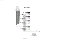
About half of the RR6 computer consists of registers. The registers are
resettable latches like shown in the diagram above, but instead of
having just one relay to store a logic 1 or 0 they have six relays that
store six bits of information. These six bits can represent a number in
the range 0 to 63. The registers pass patterns of six bits from one to
another through six wires called a bus.

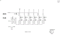
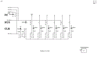
The diagram above shows two registers connected to the bus. A number (or
bit pattern) in the left register is copied to the right register like
this:
The gate relay in the left register is activated by a control signal
that closes its contacts, connecting the register's latch relays to the
bus. This puts the number stored in these latches onto the bus.
The receiving register at the right first gets a pulse on its clear relay
to reset its latches to all zeros (000000). Next, its gate relay is
activated. This connects its latches to the bus, making them match the
number on the bus. Thus the number is copied.
Decoder
Under Instruction Set on the main page, two steps are shown for each
instruction. For instance, the Clear (CLR) instruction sets the transfer
register (TR) to zero on its first step, and on its second step TR is
copied into the register (REG) selected by the three "rrr" bits in the
instruction.
        CLR     00 100 rrr

        1.      TR <- 0
        2.      REG <- TR
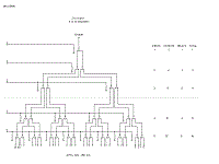
The three "rrr" bits select one of eight registers using a decoder
circuit. The three binary digits are decoded into one of their eight
possibilities.
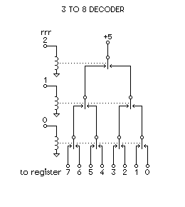
The diagram above shows the three "rrr" bits connected to the three
inputs at the left. This activates one of eight outputs at the bottom.
Each output connects to a gate relay on a register, thus selecting it to
be connected to the bus. In the case of the CLR instruction the selected
register gets zeros copied into it by TR.
ALU
The Arithmetic Logic Unit is perhaps the heart of the computer. It's
where all the computations are done. It adds and subtracts, and it does
the (bitwise) logic functions AND, OR, XOR, and NOT. The basic design is
from
here. The diagram below shows how the ALU is wired for one of the
computer's six bits.
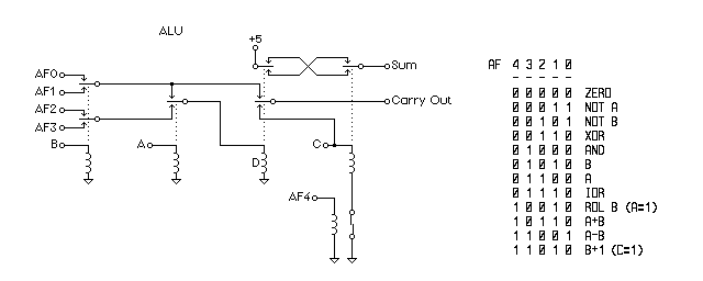
The terminals labeled Sum and Carry Out indicate its ability to add a
pair of bits on input terminals B and A along with a carry-in on C. The
terminals labeled AF0 through AF4 select the function to be performed.
The table to the right shows the configuration of these AF inputs for
each function.
Because this circuit is somewhat difficult to understand, simplified
equivalent circuits are shown below, starting with when the NOT A
function is selected.

The NOT A function complements the A input. That is, the output S is 0
when A is 1 and vice versa. Since just AF0 and AF1 are set "true" for
this function, the circuit can be redrawn with their signals connected to
+5 volts while the other inputs are unconnected.
This makes it apparent that the B input has no effect, so the drawing can
be further simplified as shown to the right. There, it's apparent that
the D relay is activated when the A relay is not, and vice versa. Since
the S output is the same as D, S is equal to NOT A.
What about the CO output? It's connected to the C input on the next
higher bit place (not shown), but since C has no effect on the S output,
the output on CO also has no effect.
The ADD A+B configuration is shown below. The table to the right
shows all possible combinations of inputs A, B and C and how they affect
relay D and outputs S and CO.
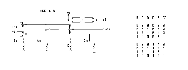
Note that D only depends on A and B (D = A^B). If there is no carry-in at
C then S is the same as D. If there is a carry-in then S is the complement
of D. Thus S is the same as adding A+B with carry-in C.
The CO output? If relay D is activated then CO is the same as C, and if D
is not activated then CO is the same as B. Thus CO is the Carry Out for
A+B.
A similar analysis confirms the other operations of the ALU.
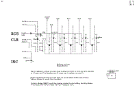
INC
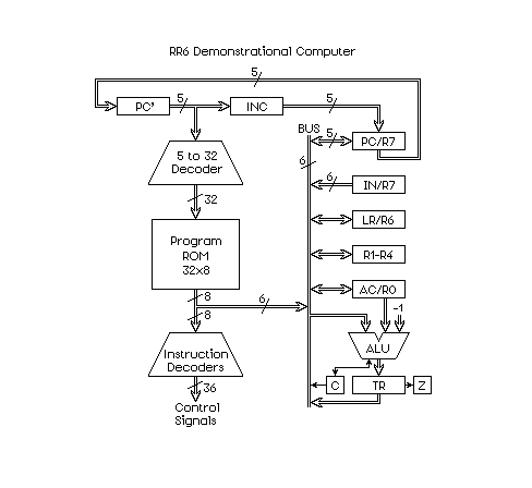 The INC box shown in the block diagram at the right is an
adder circuit similar to the ALU adder. It increments the program
counter (PC) by adding a 1 (or 2 for skips).
Executing instructions
Registers, decoders and the ALU combine to make a device that can
automatically execute instructions as follows:
The program counter register (PC) is copied to an internal register
called PC' (which is not accessable by programs). PC' holds the address
of the instruction being executed while PC (R7) gets modified to hold
the address of the next instruction to be executed.
As can be seen in the block diagram, the output of PC' goes to a decoder
that converts its five bits to select one of 32 locations in the program
memory. The PROM outputs the 8-bit instruction for the selected address.
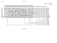
These eight bits go into the instruction decoders that select one of 26
instructions and one of eight registers for the instructions that have
"rrr" bits. The instruction decoders also output control signals to
configure the ALU for the instruction's operation and to select which
register provides the numeric value for the operation.
For example, the ADD instruction outputs the AF1, AF2 and AF4 signals to
configure the ALU for the ADD operation. It also outputs "rrr" bits, such
as 011 to specify that the number stored in register R3 is to be sent out
on the bus where it can be added to the number in AC. The sum is then
latched into the transfer register (TR).
This all occurs on the first step of the instruction. On the second step
the sum in TR is sent out on the bus, AC is cleared, and its gates are
closed. Thus the sum is stored into AC.
Two additional control signals enable gates that latch the states of the
carry output (C) and the zero status (Z) bits.
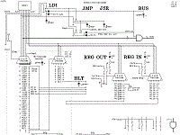
Schematics
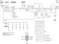
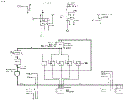
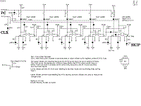
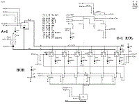
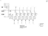
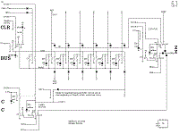
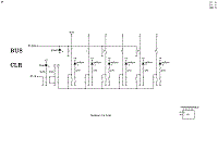
The exact details of how everything works is shown in the following
drawings.
Resistors for limiting the current through LEDs were determined by
adjusting them to get the desired brightness. The green LEDs have a
built-in resistor appropriate for 5 volts.
The RC (resistor-capacitor) values for the oscillator on the CLOCK/R7/IN
board were calculated, then adjusted for best performance. The 22uF
capacitor on this board was added to fix a timing glitch. Its value was
determined by experiment.


Back to the RR6 main page
Last update: 27-Sep-2019
